B.S. Project
|
|
- The Total Ionizing Dose will result in the charge build up in the gate dielectric(SiO2 for example) bulk and the interface between the dielectric and semiconductor materials(Si for example.)
- The charge build up will change the transistor characteristics, such as the threshold voltage and the leakage current.[1]
[1]Andrew Holmes Siedle, and Leonard Adams, “RADFET: a review of the use of MOS devices as integrating dosimeters”, Radiat. Phys. Chem. Vol.28, No.2,pp.235-244, 1986
|
- To remain high sensitivity to TID, the oxide thickness must be large
- As technology scaling continues, the oxide thickness is very thin, indicating it being poor candidate for TID monitor
- The Buried Oxide in SOI technology could be a good alternative
|
|
|
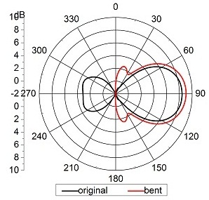
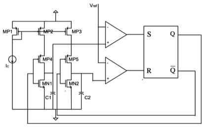
The circuit diagram: |
|
|
- The basic idea is to measure the off-state leakage current after the TID exposure
- By converting the current into periodic wave through the CCO, and measure the frequency through the digital circuit
- The relationship between the leakage current and the TID exposure could be used as an indication of the dose level[2]
[2]Marty R. Shaneyfelt,etc. “An Embeddable SOI radiation sensor”, IEEE. Tran. Nucl. Sci., Vol. 56, No. 6, pp. 3372-3380, Dec. 2009
|
- The CCO input range of 10nA~100uA, a broad range
- The double capacitor scheme is used here, that the period is the sum of the charging time of C1 and C2
- Free from the problem of matching the charge and discharge current encountered in single capacitor scheme
|
|
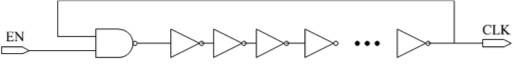
| On-chip Clock: due to the low single stage delay in 32nm IBM SOI technology, it 's hard to get a 1MHz oscillation. Some methods have to be taken |
Traditional current starved stage
|
Single stage delay of traditional current starved stage |
- The bias "ContN" and "ContP" are used to control the current
- Increase the single stage rise and fall time
|
- Single stage delay is 180ps
- It needs 2771 stages to get 1MHz oscillation
- Not applicable, need to improve
|
Improved single stage
|
Single stage delay of improved single stage |
- The bias "ContN" and "ContP" are used to control the TG gate to increase delay instead of the charging and discharging current
- MOS transistor acting as capacitor at the output node
|
- Single stage delay is 273.5ps
- It only needs 401 stages to get 2MHz
|
On-chip clock
|
|
- The clock signal is 1MHz periodic wave
- The on-chip and off-chip clock are used. For the on-chip clock, the ring oscillator is chosen. The off-chip clock will be implemented by quartz crystal
|
- showned here is an example of the ring oscillator output. The frequency is 50MHz
|
|
| Traditioanl CCO design |
Improved double capacitor CCO design |
- Relies on the matching of charging and discharging current
- The control circuit to switch between charging and discharging mode is difficult
- The oscillation period equals to the sum of charging and discharging time
|
- does not rely on the matching of charging and discharging current
- relies only on the matching of charging current of the two capacitors, implemented by current mirrors
- high linearity range
|
|
|
- Shown above is the diagram that shows the voltage on the two capacitors
- The oscillation period Tc is the sum of the two capacitors charging time
|
- shown is an example of the output. The input current is 100uA, and the oscillation frequency is 1GHz
|
| f-I relationship on a lienar scale |
f-I relationship on a log-log scale |
- Due to the fixed delay of the control circuit, the frequency tends to saturate at high input current
- it shows power law
|
- on a log-log scale, it is quite linear, confirming that it is a power law dependence
|
|
Overall result |
|
- Shown here is an example of the behavior of the overall circuit
- Test condition: clock frequency--2MHz; input current--100nA;
- The CCO output frequency is 43.4MHz, so the output should be 22, namely (000000010110)2
|
|
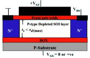
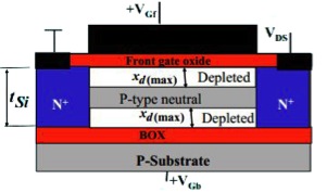
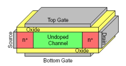
Planar SOI
  |
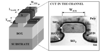
Non-planar SOI
|
- Shown above is two kinds of planar SOI transistor, Partially Depleted(PD) and Fully Depleted(PD) transistor, based on the fact whether the body is fully or partially depleted.
- SOI transistor reduces the parasitic capacitance and alleviates the short channel effects
- The Buried Oxide(BOX) is unique to SOI technology, which is utilized in the TID monitor project above[3]
[3]K.N.Bhat, “Silicon On Insulator Devices”, E3-327 Nanoelectronics Devices lecture series Lecture #23, Oct. 2007
|
- The non-planar SOI transistor is characterized by more than one gate around. Shown above is two examples of dual gate and triple gate SOI. And the right is an Omega-gate FinFET.[4-5]
- Non-planar SOI transistor shows better gate control over the channel, which indicates better electrical characteristics.
[4]Kavitha Ramasamy, ”Double-Gate MOSFETs”, Cristina Crespo, Portland State University, 2003
[5]M.Gaillardin, etc. “Total Ionizing Dose Effects on Triple-Gate FETs”, IEEE, Trans. Nucl. Sci. Vol. 53, No. 6, pp. 3158-3165, Dec. 2006
|
BG FG |
|
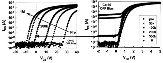
- Shown above is the TID response of FD SOI transistor biased at OFF state
- There is an increase of leakage current of the Front Gate transistor
- A large threhold voltage shift at the Back Gate transistor
- For the FD SOI transistor, because of the electrical coupling between the FG and BG transistor, it is more complicated. Detailed information could be found in the review paper[6]
[6]J.R.Schwank, V.Ferlet-Cavrois, M.R.Shaneyfelt, P.Paillet, and P.E.Dodd, “Radiation Effects in SOI Technologies”, IEEE, Trans. Nucl. Sci. Vol. 50, No. 3 pp. 522-538, Jun. 2003
|
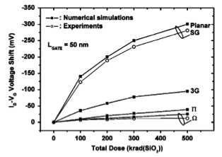
- As shown is the threhold voltage shift in different non-planar SOI transistors.
- It is shown that the Triple Gate structure overweighs the other structure in terms of the TID response, because they could provide better gate control over the channel[5]
|
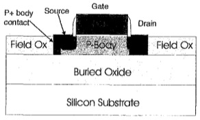
TID hardening of SOI(BUSFET)
|
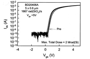
BUSFET resonpse
|
- The structure shown above is the Body Under Source FET. If charge trapped in the BOX, the interface between the body and BOX will be inverted
- But the source is above the body, so source and drain is isolated at the interface, thus enhancing the immunity to the TID exposure[6]
|
- Shown above is the TID response of the BUSFET structure
- up to 2Mrad(Si), the threhold voltage shift and the leakage current increase is negligible, showing the hardening to TID exposure
|
|
This project is finished this semester. Up to now, theory is explained and paper has been submitted. It includes several different parts.
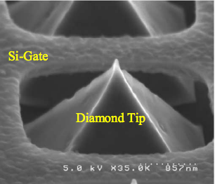
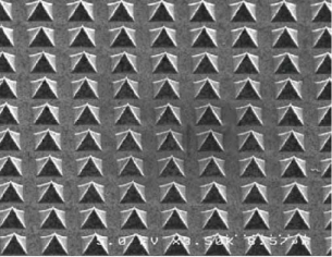
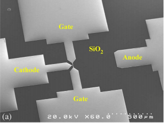
- Nanodiamond based Vacuum Field Emission Microelectronics
- Nanodiamond is a good cold electron emitter
- Two types of VFEM are proposed: vertical and lateral, as is shown in the figure below
- It shows numerous advantage over the solid state devices, such as junction free structure, temperature and radiation tolerant, higher electron mobility limited by the speed of light, higher thermal conductivity, simplicity to make, etc.[7-8]
- [7]Weng P. Kang, Tim Fisher and Jim L.Davidson, "Diamond Microemitters-The new Frontier of Electron Field Emissions and Beyond", New Diamond and Frontier Carbon Technology, Vol.11, No.2 2001, pp.129-146
- [8]Karthik Subramanian, Weng Poo Kang, and Jim L. Davidson, "A Monolithic Nanodiamond Lateral Field Emission Vacuum Transistor", IEEE Electron Dev. Lett. Vol.29, No.11, Nov. 2008,pp.1259–1261.
|
  |
 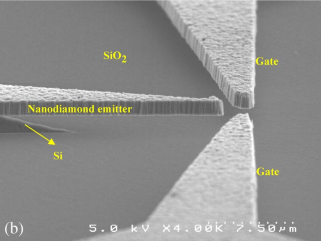 |
- Nano-gap Nanodiamond Field Emission Diode modeling and Characterization
- The first report of nanogap nanodiamond field emission diode
- Three different conduction mechanisms are reported: the Fowler-Nordheim Field Emission theory, the Space Charge Limited Current, and the Thermal Field Emission. Experimental data are modelled and verified with corresponding mechanisms.
- Different mechanisms are explained through the band diagram.
|
|
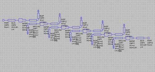
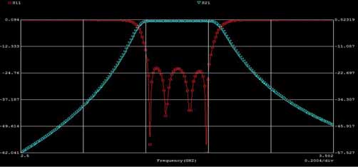
| 1.a bandpass filter implemented by coupled microstrip(5% relative bandwidth, center frequency 3GHz, return loss in-band>20dB, attenuation at 3.8GHz>20dB) |
|
|
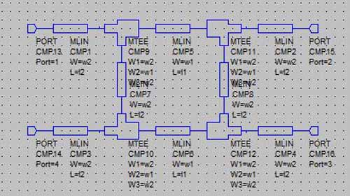
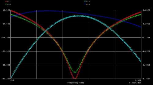
| 2.a 3dB power divider implemented by branch line(5% relative bandwidth, center frequency 3GHz, return loss in-band>25dB, isolation>25dB) |
|
|
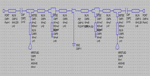
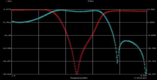
| 3.a power amplifier(10% relative bandwidth, center frequency 3GHz, return loss in-band>15dB, gain in-band>9dB and fluctation in band<1dB) |
|
|
Paper review and presentation about the performance of all kinds of fractal antennas and arrays back to top
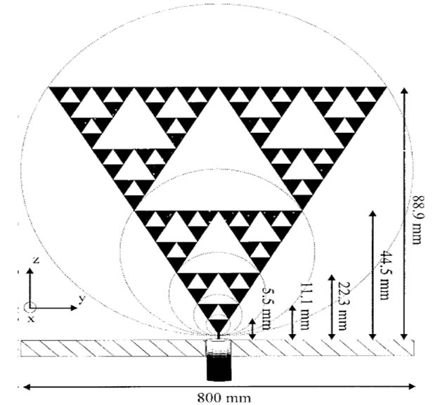
a five-iteration Sierpinski monopole |
 |
|
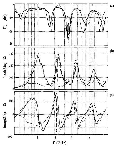
Above is one typical fractal antenna, Sierpinski fractal antenna. And next to it is the electrical parameters of it. From that, it presents a log-periodic behavior with
five bands approximately spaced by a factor δ=2. The antenna keeps a notable degree of similarity through the bands.
|
Research in the relationship between the electrical performance and its geometry structure back to top
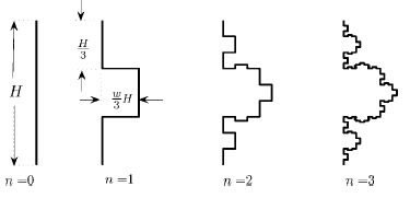
Minkowski fractal with different iterations |
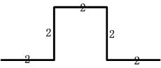
the first iteration |
 |
|
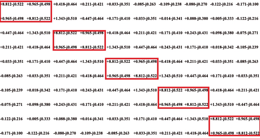
| Figure above in the right shows the impedance matrix with MoM. And the red squre frame is the impedance matrix of every basic segment. Apparently, it is a symmetric matrix. To dig the characteristic of this matrix,different methods, direct comparition of matrix element or matrix eigenvalue and eigenvector of the same or consecutive iteration level of proportionable size. |
Applied fractal geometry in Yagi-Uda antenna to decrease antenna size. Designed, simulated and optimized parameters. back to top
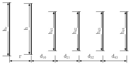
1. General Yagi-Uda antenna
|
|
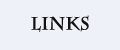
| hr |
0.51λ |
r |
0.25λ |
| h |
0.48λ |
d10 |
0.3λ |
| hd1 |
0.40λ |
d21 |
0.3λ |
| hd2 |
0.40λ |
d32 |
0.3λ |
| hd3 |
0.40λ |
d43 |
0.3λ |
| hd4 |
0.40λ |
|
|
|
|
The figure left shows the structure of general Yagi-Uda antenna. The middle one is the radiation pattern of this antenna with specific geometry size in the table
right to it. In the middle figure, different colors represent different director spacings between each other. |
2. Fractal Yagi-Uda antenna
Pictures above shows the structure of fractal Yagi-Uda antenna |
|
|
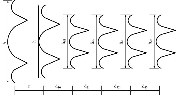
Figure above in the left shows the structure of fractal Yagi-Uda antenna. In the right is comparation of radiation pattern of fractal Yagi-Uda antennas. Different colors represent different situations as illustrated by the legend. From this, the decrease of antenna size is possible without much sacrifice of antenna performance |
|
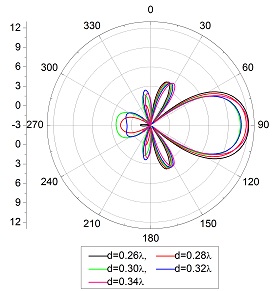
To further expand the space for decrease in size of horizontal direction, the simulation of different director spacing is conducted. The left is the resut, from which further decrease of size is possible with little sacrifice of antenna performance |
Also, to decrease the height, the simulation of different heights of array elements is conducted. the right is the result. Decrease in height results in fall in gain, which is opposite to the will. |
|
|
3. Tortuous Fractal Yagi-Uda antenna
|
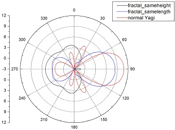
This is the radiation pattern comparition between tortuous fractal and general fractal Yagi-Uda antenna with the same height and spacing. From this, one striking advantage is the decrease of back lobe, which is just the purpose of the design. |
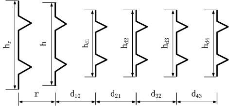
4.Smoothly curved Yagi-Uda antenna
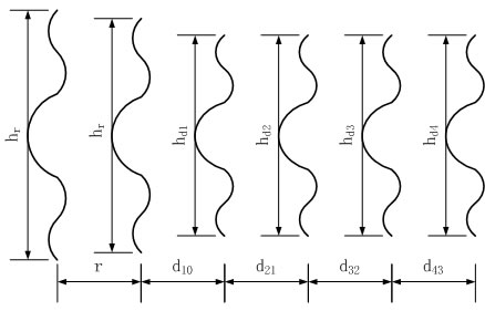
Figure above shows the structure of smooth curved fractal Yagi-Uda antenna |
|
|
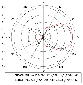
It is the comparation of radiation pattern of Koch Yagi-Uda antenna and the smoothly curved Yagi-Uda antenna. From this, it is clear that an improvement of
gain and suppression of back lobe is achieved. |
|
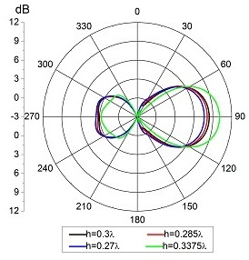
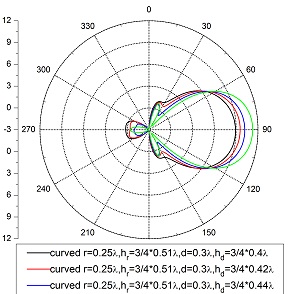
To observe the influence of director height has on the performance of antenna, different director heights have been simulated. From the result, it is clear that the long height is favorable to achieve high gain. |
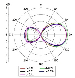
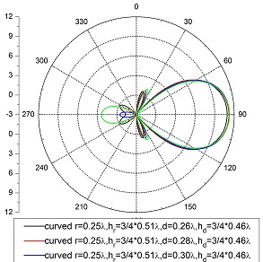
To observe the influence of director spacing has on the performance of antenna, different director spacings have been simulated. From the result, it is obvious that director spacing has little impact on the forward gain, but on the back lobe.
|
 |
|
| |